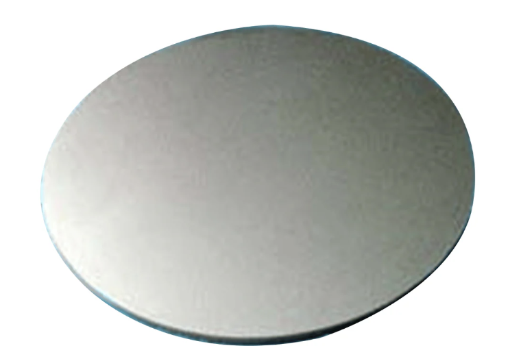
High Purity Germanium Wafer is a premium-grade semiconductor substrate specially engineered for advanced electronics, infrared optics, and radiation detection applications. Made from ultra-pure germanium (Ge), it offers superior electrical properties, high carrier mobility, and precise thermal stability.
 The high purity germanium wafer delivers exceptional performance in infrared detectors, solar cells, gamma-ray detectors, and high-speed electronic devices. Its defect-free crystal structure and tight dimensional tolerances ensure accurate fabrication and reliable device operation.
 It is extensively used in industrial and laboratory environments where a contamination-free setting and high precision are critical. For a reliable, high-quality, and precision-engineered semiconductor substrate, the High Purity Germanium Wafer offers the perfect combination of performance, consistency, and long-term efficiency.
Germanium Wafer
- High Purity Material – Made from premium-grade High Purity Germanium Wafer, ensuring superior performance for advanced semiconductor and optoelectronic applications.
- Exceptional Electrical Properties – Offers excellent electron mobility, low defect density, and consistent conductivity for precise electronic devices.
- Precision Surface & Flatness – Polished wafer with smooth surface, uniform thickness, and tight tolerances for high-precision semiconductor fabrication.
- Excellent Thermal Stability – Maintains structural integrity under high-temperature processes and operational conditions.
- Versatile Industrial Applications – Ideal for infrared optics, photodetectors, semiconductor devices, high-speed electronics, and solar cells.
- Reliable & Long-Lasting – Ensures minimal defects, consistent performance, and high yield in critical electronic and optoelectronic applications.
- Customizable Specifications – Available in various diameters, thicknesses, and orientations to meet specialized industrial requirements.
- High Purity Material – Made from premium-grade High Purity Germanium Wafer, ensuring superior performance for advanced semiconductor and optoelectronic applications.